
Introduction:
This is an article about how to use Langer ESA1 set Solve the problem of radiation emission of electronic products using the guide, electronic products PCB EMI radiation emission problem has always been the focus of hardware developers, now let us through the ESA1 set and the far-field test data in the darkroom to illustrate how to solve the problem of radiation emission, this product by the Shenzhen EUTTEST agent sales and provide after-sales service.
Rectification case:
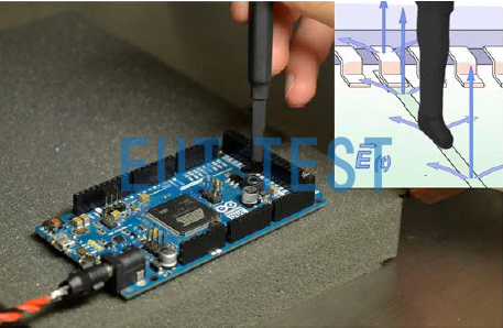
The PCB (DUT) to which we are trying to troubleshoot the radiated emission exceedance is a microcontroller board with two cables connected.
The first cable is used for power supply and the second is used to connect to the auxiliary device via the serial interface as shown below:
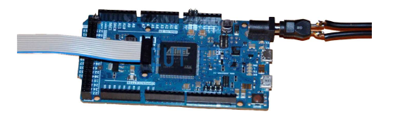
PCBs with excessive radiation emission faults
First test the far-field test data:
We need to first obtain a spectrogram of the DUT's far-field radiated emission in a radio-wave darkroom or shielded room, which is the goal of our rectification.

Testing of radiated interference from DUTs using radiated emission test antennas in an airwave darkroom
Test completed:
Upon completion of the test, as shown in the figure below, the DUT's radiated emission level exceeded the limit line at several frequency points distributed over the 30MHz-1GHz range, and our goal was to keep the red curve in the figure below 6dB+ below the limit line.
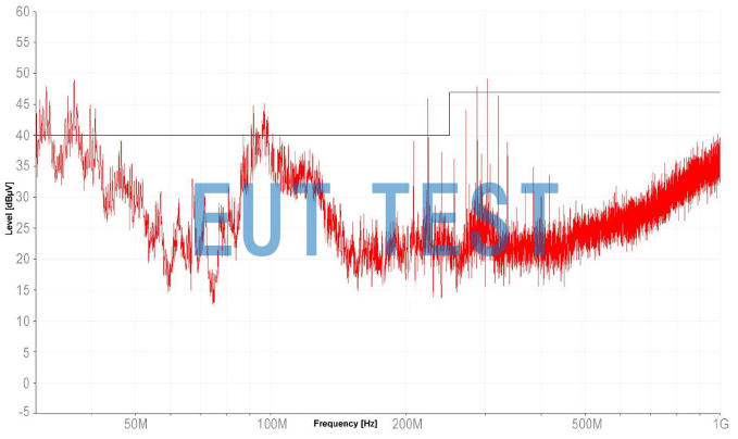
The radiated emission level of the DUT exceeds the limit line requirement
The EUT test spectrum above shows multiple limit violations.Langer EMV-Technik GmbH's ESA1 kit for troubleshooting can be set up directly at the hardware designer's desk, eliminating the need to return to an expensive third-party testing lab for far-field lab measurements.
Begin rectification:
Step 1: Retesting
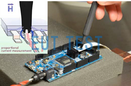
As shown in the figure below, the circuit board of the DUT under test is placed on the bottom board of a shielded tent and power is supplied to the DUT through the HFW 21. The HFW 21 is an RF current transformer, also called a current probe. It measures the high-frequency excitation currents from the DUT's power cable that cause the antenna (consisting of the cable and PCB) to radiate.
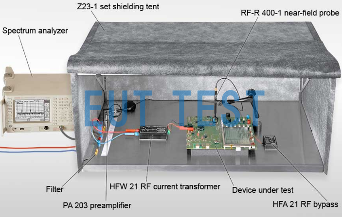
Place the circuit board of the DUT under test on the base plate of the shielding tent.
The tent's tarp was then closed, and an external spectrum analyzer or receiver was used to perform a 30MHz-1GHz sweep test The measured spectrum was recorded with the tent closed, and since one was a far-field test and the other was acurrent probetest, so we get a new spectrum plot that is slightly different from the transmit spectrum measured by the antenna. However, the two measurements are proportional.
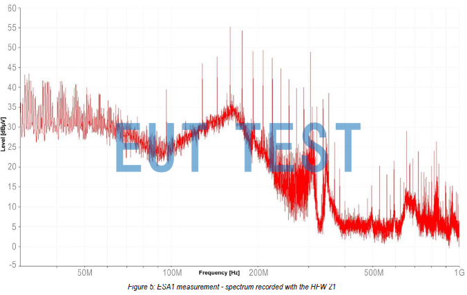
Spectral plots from the HFW 21 current probe in the ESA1 set are proportional to the far-field test results.
Step 2: Investigation and modification
Once we have the new spectrum of radiated emissions, in order to locate which RF sources on the DUT these emissions are coming from, we need to locate the exact position in the Z23-1 open shielded tent using a near-field probe. The ESA1 set offers a large number of near-field probes with different resolutions and test frequency ranges, but of course, you can use any other near-field probe already available, as the system is open. You can of course use any other near-field probe you already have, as the system is open.
Localization of emission sources using different near-field electric field probes
When scanning the test with an electric field probe above the PCB and finding a similar spectrum to the first step of the test, we can confirm that the DC/DC converter here is emitting radiated emissions into the environment. To confirm this assumption and to reduce the E-field coupling, we place a shield, i.e. a conductive copper foil, over the coil of the DC/DC converter and connect it to the GND ground point of the PCB.
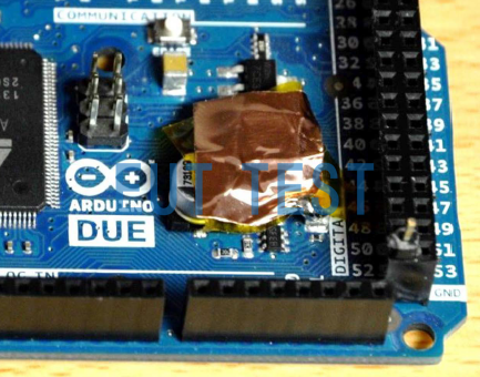
Placement of a shield on the coil of the PCB's DC/DC converter
Use the same method to locate all high level frequency points and take action.
Next we use the near-field magnetic field probe to identify the clock line of the serial interface in the ribbon cable of the DUT as a source of interference. Spikes in the interference level can be seen in the frequency range between 200 MHz and 400 MHz, corresponding to the frequencies in the far-field antenna measurement.
Using a near-field magnetic probe to identify the clock line of the serial interface in the ribbon cable of the DUT as a source of interference
In order to reduce this disturbing signal, we use a 47pF capacitor added to the clock signal line of the DUT.
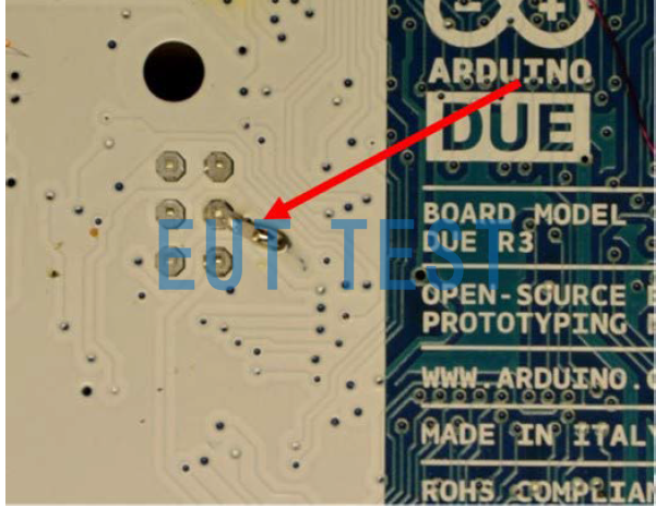
Add to the clock signal line of the DUT with a 47pF capacitor
Step 3: Verify the effectiveness of EMI rectification
The validity of the modification was checked by measuring again with HFW 21 in the closed tent, and as can be seen in the figure below, the intensity of the high frequency excitation current in the power line was successfully reduced. The shielding of the coil mainly reduces the broadband interference, while the added capacitance to ground on the clock line reduces the intensity of the radiated interference level. With this knowledge, another antenna measurement can now be made.
Two effective ways to solve electromagnetic interference EMI
Sources and differences between conducted and radiated interference
The red curve in the figure below represents before the modification and the blue curve represents after the modification.
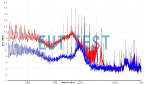
Radiated Emission Interference Spectrum before and after Rectification
Next we perform another far-field test, and as you can see from the blue curve in the test results below, the DUT that was exceeding the limits just a few moments ago is no longer exceeding the radiated emission limit line. So all we had to do was quickly find a feasible implementation of the modification and the EMC problem was finally solved.
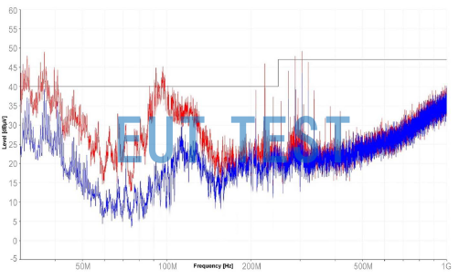
Performing the far-field test again shows that the DUT has met the limit line requirements
Summary:
As you can see from the above, Langer's ESA1 set provides a shielded environment that can be used in a common room, reduces the cost of traveling to third-party labs for testing, and increases development efficiency.
This kit is configured with a current sensor that can be connected directly to the product power supply for testing.
Multiple electric and magnetic near-field probes are also configured to help customers localize interference from large areas of the PCB to specific components.
Additional test method recommendations:
When the PCB area is very large, if it is not possible to put the DUT into the shielding tent of ESA1 set, then we recommend you to use the FLS 106 PCB set To perform automated EMI scanning, this tool measures top and bottom PCB interference separately and provides a free test software to generate 2D and 3D test reports. Of course, it can also measure small PCBs.

Perform automated EMI scanning with the FLS 106 PCB set