Evaluation of IC integrated circuit chips subjected to ESD static electricity
- Article Directory: How to test integrated circuits for electromagnetic compatibility
Introduction:
Today, new developments in electronics manufacturing are increasingly dominated by EMC requirements. The subsequent costs of product development due to the failure of electronic modules in EMC compliance tests are considerable. The integrated circuits used in an electronic system play a decisive role in its overall EMC performance. ICs are often the cause of interference emissions or immunity weaknesses, and it is difficult to control them in such cases.
Over time, ICs have become smaller, which results in higher switching rates and the need for lower supply voltages. Due to these two factors, ICs become more susceptible to ESD.
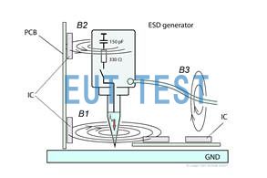
Figure 1 Current pulse injected into the device under test using an ESD gun.
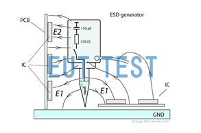
Fig. 2 A magnetic and an electrical interference field are induced.
Injection of IC under test using ESD static gun
Electronic equipment is tested using an ESD generator (ESD gun) during EMC conformance testing according to IEC 64000-4-2. The ESD generator produces the current pulses required by the standard (Figure 3), injected into the device under test ((Figure 1)The ESD pulse couples into the metal parts of the electronic device and moves from there to the IC through conductive and capacitive/inductive coupling.) This ESD pulse couples into the metal parts of the electronic device and from there moves to the IC through conductive and capacitive/inductive coupling. the amplitude of the interference pulse varies with time along its path to the IC. The purpose of this report is to examine the coupling path of the IC. The amplitude of the interference pulse affecting the IC is measured as a function of time for each coupling path. This helps to determine which couplings are relevant and which parameters (rise time, voltage strength, waveform, amplitude, current, voltage, electric or magnetic field) have an effect on the coupling. These findings allow the development of selected EMC countermeasures to protect the IC.
The ESD generator senses magnetic and electric field disturbances:
In addition to compliant current pulses, the ESD generator senses magnetic and electric fields (Figure 1, Figure 2). As a result of the discharge current, a magnetic eddy current field is generated at the tip of the ESD generator, which rotates in the line network of the IC and module. An interference voltage is induced in the conductor circuits penetrated by the magnetic field. This voltage is superimposed on the electrical signals of the electronic system and leads to malfunctions in the electronic equipment.
The inductor is integrated in the tip of the ESD generator. The discharge current from the ESD gun causes a voltage drop across this inductor. This voltage drop generates an electric field E1, which emerges from the tip of the generator and extends through the lines and ICs into the device under test (Figure 2). As a result, interfering current pulses are transmitted to the lines and ICs, causing malfunctions in the electronic equipment.
In addition to the interfering currents emitted through its tip as described in the standard, electric and magnetic fields occur in the body of the ESD generator ((Figure 1, Figure 2)). When compared as a function of time, these fields may be quite different from the interference events described by the standard. These fields have additional interference effects on electronic equipment that may exceed the desired effects caused by tip interference. The extent to which these fields interfere with electronic equipment depends on the position of the ESD generator relative to the equipment module. Weaknesses in the equipment may respond purely by chance when the ESD generator is turned and tilted. Functional failures of electronic devices seem to occur in a chaotic manner. Developers can no longer understand and analyze cause and effect.
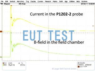
Fig. 3 Current variation with time for interference triggered by ESD generator (top)
Magnetic flux density near the tip of the ESD generator (bottom)
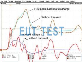
Figure 4 Module
ESD generator first discharge peak current induced voltage in ESD gun current loop und : NSG435
Voltage: 2 kV
Figure 4The first peak discharge current of the ESD generator is shown in magnified form. Several transients are clearly visible on the leading edge and are designated as ESD transients in the following. The peak discharge current and the ESD transients also produce the same flux B1 with time (Figure 1). The magnetic flux B1 induces an interference voltage uind the conductor circuit of the electronic module (Figure 4The size of the conductor circuit is 8 mm2 .) The size of the conductor circuit is 8 mm2 . the voltage of the ESD generator is set to 2 kV. in addition.Figure 4It is clearly shown that the largest voltage inductions are generated by ESD transients. The standard-defined rise time of 0.7 to 1 ns peak discharge current produces a lower disturbance voltage induction (Figure 4(There are no transient curves).
The ESD transients of an ESD generator have a stronger disturbance effect than the peak discharge current. Therefore, the standard-defined waveform parameters are not suitable for a full description of the disturbance effects of ESD generators. The transients are very much dependent on the type of ESD generator used in practice.
Fields B2 and B3 enhance the interference effect of the ESD generator (Figure 1).Figure 5The interference voltage induced by magnetic field B2 in an 8 mm2 conductor loop is shown. The voltage variation with time is quite different from the usual curve of a known ESD event. The 200 ps wide spike has the greatest disturbance effect on the IC, with an amplitude of 4.8 V. This pulse is too short for the slower older generation ICs and will cause little or no disturbance. Its amplitude is 4.8 V. This pulse is too short for slower, older-generation ICs to cause any problems. Modern, fast ICs can handle such narrow pulses and fail. The special thing about this event, the voltage induced by the field B2, is that it is not related to the standard pulse. It occurs outside of the actual test, which means that the standard test is no longer definitive.
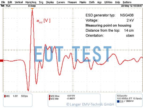
Fig. 5 Voltage induced in an 8 mm2 conductor loop by field B2 generated by the ESD generator housing.
Figure 6Shows the principle of operation behind voltage induction (equivalent circuit) through the magnetic field B of an ESD generator. The induction loop can be located outside the IC on the printed circuit board or inside the IC package. In this example, it is formed externally by a trace that is grounded through a low impedance driver. Interference voltages enter the IC through conductive coupling through the traces. inside the IC, the sense loop consists of pins, leadframes, and bonding wires. The voltage uin induced in the sense loop appears at the input of the IC. Both internal and external voltages can cause failures inside the IC. The voltage uind depends on the discharge current of the ESD generator and the rate of change of the magnetic field, respectively. This correlation is described by the law of induction: uind = -d Φ / d t. The faster the rate of change of the disturbance, the higher the induced voltage. Burst generators according to IEC 64000-4-4 provide pulses with a rise time of 5 ns. The magnetic field of the burst generator induces a lower voltage than the disturbance voltage generated by the ESD generator. the ESD generator delivers pulses with a rise time of 0.7 to 1 ns and induces a voltage five times higher for the same value of current. the ESD generator's leading-edge transients have a rise time of about 200 seconds. These transients induce higher voltages.
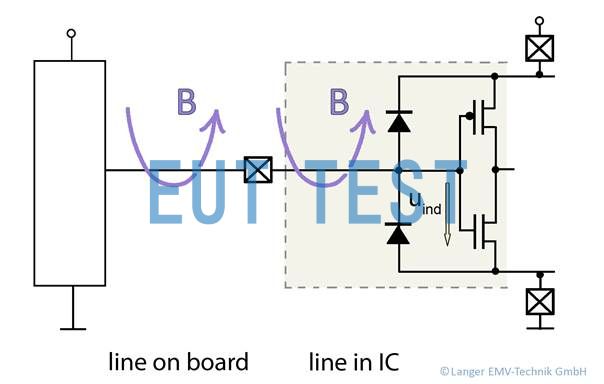
Figure 6 Voltage induced by the magnetic field of an ESD gun on the conductor loop of an electronic module or IC.
Figure 7This correlation is shown. The current shown here produces a magnetic field across the conductor loop B. The voltage uid is induced in the conductor loop. Interference events: bursts, ESD, ESD transients induce different voltages. The width of the induced voltage pulse corresponds to the rate of change of the current. A pulse of 5 ns width is generated during a burst event, a 1 ns width for an ESD event, and a 200 ps width for an ESD transient. Modern ICs will also handle pulses 200 ps in width, which can lead to IC failure or even complete failure.
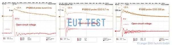
Fig. 7 Voltages induced in the 8 mm 2 conductor loop during a disturbance event: burst, ESD, ESD transient
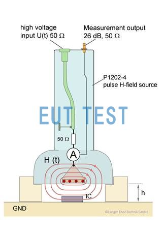
Fig. 8 Test setup for determining IC immunity to magnetic field interference
According to the law of induction, the value of the induced voltage is inversely proportional to the rate of change of the disturbing event.Figure 7The measurements were performed using defined field sources (Figure 8). These field sources have a fixed field generation geometry for different disturbances. Therefore, the test current will always generate the same field coupling so that measurements can be compared for the three interference events described. the IC can withstand the defined fields and their immunity tests in operation.
During the discharge process, high rate of change switching voltages occur at the high voltage switches, current conductors, and other components in the ESD generator (Figure 2). These switching voltages produce a high rate of change of the electric field coupled from the generator enclosure to the device under test.Figure 9Shows the electric field generated from the rear of the ESD generator enclosure. The rate of change is about 1 nanosecond.
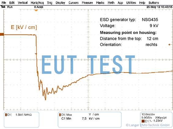
Fig. 9 Electric field at the rear of the NSG435 ESD generator at 9 kV.
Figure 10Shows the equivalent circuit diagram and the principle of operation behind the ESD generator electric field coupling. The electric field is coupled into the signal line. The capacitive coupling between the affected signal line and the ESD generator is low. The value of this capacitance depends on the surface area of the signal line and is within the fF range of this coupling. the electric field of the ESD generator drives a capacitive current into the signal line. This current flows to ground (GND) through a pull-up resistor or the internal resistor of the connected driver. The current generates a voltage pulse across the resistor. The peak value of the voltage pulse depends on the rate of change of the electric field, the pull-up resistor and the surface area of the signal line subjected to the electric field. The width of the pulse depends on the rise time. The faster the rate of change of the disturbance, the higher the voltage at the coupled input. Pulse generators according to IEC 64000-4-4 provide pulses with a rise time of 5 ns. The voltage coupled to the E-field of the burst is lower than that of the disturbance triggered by the ESD generator. the ESD generator delivers pulses with a rise time of 0.7 to 1 ns, and couples a voltage five times higher into the device under test. The maximum rate of change of the E-field from the ESD generator is about 200 seconds. As a result of these events, higher voltages are coupled into the device under test. The higher the voltage of the coupling input. Burst generators according to IEC 64000-4-4 provide pulses with a rise time of 5 ns. The voltage coupled to the electric field of the burst is lower than the interference triggered by the ESD generator. the ESD generator delivers pulses with a rise time of 0.7 to 1 ns and couples a voltage five times higher into the device under test. The maximum rate of change of the E-field from the ESD generator is about 200 seconds. As a result of these events, higher voltages are coupled into the device under test. The higher the voltage of the coupling input. Burst generators according to IEC 64000-4-4 provide pulses with a rise time of 5 ns. The voltage coupled to the electric field of the burst is lower than the interference triggered by the ESD generator. the ESD generator delivers pulses with a rise time of 0.7 to 1 ns and couples a voltage five times higher into the device under test. The maximum rate of change of the E-field from the ESD generator is about 200 seconds. As a result of these events, higher voltages are coupled into the device under test.7 to 1 ns and couples five times higher voltages into the device under test. The maximum rate of change of the E-field from the ESD generator is about 200 seconds. As a result of these events, higher voltages are coupled into the device under test.7 to 1 ns and couples five times higher voltages into the device under test. The maximum rate of change of the E-field from the ESD generator is about 200 seconds. As a result of these events, higher voltages are coupled into the device under test.
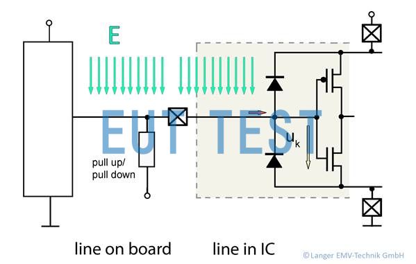
Figure 10 Coupling the E-field into the conductors of an electronic module or IC
This electrical coupling was investigated in experiments. These experiments used theAs shown in Figure 8A similar test setup is shown.E The field source is used to generate the required fields.Figure 11The results are shown.5 ns burst pulse and 200 ps ESD pulse were used for the measurements. The dependence on the pull-up resistor (driver) used in the setup was also checked.
The voltage coupled to the IC is proportional to the pull-up resistor. The lowest voltage (0.15 V) is coupled to the IC with a 5 ns rate of change and a 50-ohm pull-up resistor, which does not yet interfere with the IC. The highest voltage is generated with a 200 ps rate of change and a 10 kOhm pull-up resistor to 64 V. The lowest voltage (0.15 V) is coupled to the IC with a 5 ns rate of change and a 50-ohm pull-up resistor.Figure 11The 200 ps pulse is shown to have been able to cause a malfunction in an IC that has a low impedance pull-up (driver) resistor of 50 ohms (at 3.5 V). This makes the pulse particularly dangerous for electronic circuits, since even the smallest part of the line driven by a low-impedance source (e.g., data bus, address bus, etc.) can fall victim to interference in this manner. The surface area of a test pad size on the corresponding line is sufficient to cause the IC to fail. This problem is limited to modern, highly integrated ICs that are fast enough to handle this type of pulse.
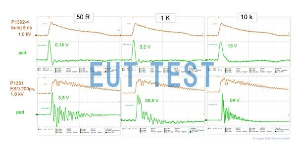
Fig. 11 Electrical coupling to a conductor as a function of the rise time of the disturbance pulse and the value of the pull-up resistor used in the circuit.
It is important for designers to understand the immunity of ICs intended for use in modules with highly integrated circuits. Not all pins of an IC are equally sensitive to EMI. There are usually only a few highly sensitive pins. These pins must be identified in order to take appropriate and effective EMC countermeasures.
For example, signal lines should be routed in the inner layer and shielded through the GND plane on both sides to minimize the interference effects of electric fields. It must be noted that the number of test pads and via holes must also be reduced.
Modern measurement techniques and test equipment can be used to determine the conducted and radiated immunity of ICs.
- Created Date: 2024-08-26 10:35:11 ;
- Last modified on 2024-08-26 18:35:11 ;