IC Reactions induced by electromagnetic field coupling of integrated circuit chips
- Article Directory: How to test integrated circuits for electromagnetic compatibility
Introduction:
The impact of EMC on chip functionality can vary widely, from brief tolerable failures (e.g., short switching of port outputs) to complete failure of the IC, i.e., permanent loss of functionality.
This paper discusses conducted interference through IC pins. In these cases, the interference enters the IC through the circuit network of the electronic board, and EMP and ESD fields originating from the electronic board environment are the cause of these conducted disturbances.
How do ESD and bursts create EMI in electronic systems?
Interference injected into electronic equipment during EMC testing generates magnetic and electrical interference fields. These fields penetrate the electronic board (Figure 1).
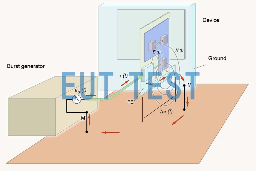
Fig. 1 Effect of burst or ESD interference on electronic boards.
Inductive coupling (B/H field)
The wiring of an electronic board forms loops relative to the ground plane. If a magnetic field now enters these loops, a voltage to ground is induced in them. If the conductor loops are connected to an IC pin, a ground induced voltage will be present on that pin (Figure 2). The induced voltage may interfere with useful signals on the signal line and drive an interfering current into the IC.
The inductive coupling has a low source impedance and drives a high strength current into the IC. current values are in the range of up to 30 A. For this to be effective, the line must be connected to ground outside the IC with a low resistance (capacitor). For low source impedance to be effective, the line must be connected with low resistance (capacitor) to ground outside the IC.
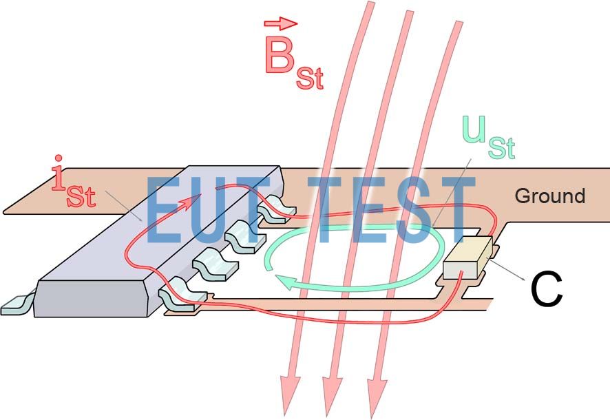
Fig. 2 Interference with a network of lines on an electronic board by means of a magnetic field.
Capacitive coupling (electric field)
The lines on the circuit board form the coupling electrodes for the interfering electric field, theAs shown in Figure 1.. The electric field couples the interference current to the line (coupling electrode). Interference currents flow to ground through pull-ups, pull-downs, or drivers and produce an interference voltage drop across them (Figure 2). Induced interference voltages are present at the IC inputs and can modify useful signals or drive interference currents into the IC. Capacitive coupling has a high source impedance and drives low strength currents into the IC. current strengths are in the range of up to 1 A. For high source impedance to be effective, the line must be connected to ground outside the IC via pull-ups and pull-downs on a high resistor (resistor R).
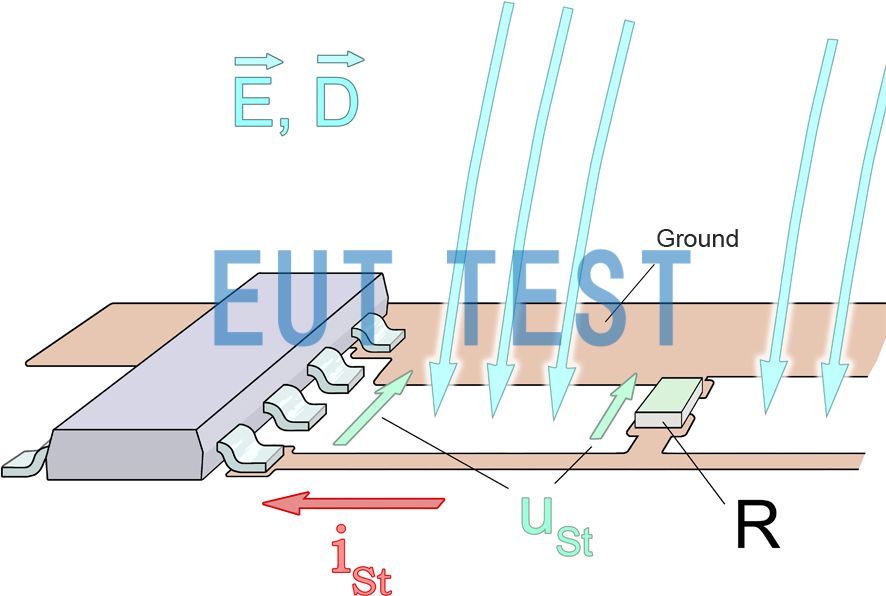
Fig. 3 Interference with the network of lines on an electronic board by means of an electric field.
IC pins with EMC characteristics for conducted interference
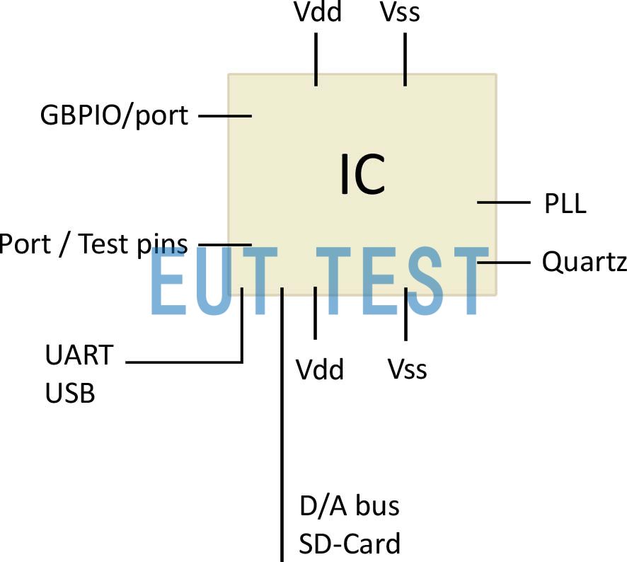
Figure 4 IC pins and their respective EMC characteristics.
Conducted interference enters the IC through its pins due to a capacitive or inductive coupling mechanism. the characteristics of the coupling mechanism and the respective characteristics of the IC electronics connected to the IC pins determine some of the cause and effect relationships. IC pins can be divided into several pin groups depending on the EMC characteristics of the connected IC electronics.
The most important groups of signal pins are:
- port pinout
- Test Pins
- Interface (USB, UART, etc.)
- bus pin
- Crystal Connection Pins
- Reset pin
- Power pins: Vdd and Vss pins
Signal Pins - IC Response to Disturbances Caused by Electric Field Coupling
The first possible reaction:
Interference voltages are superimposed on the useful signals due to capacitive coupling to the signal lines of the electronic board. The interfering voltage changes the logic state of the useful signal. When the microcontroller reads the useful signal, the following responses may occur:
- The useful signal is checked for possible interference by performing several scans in the microcontroller. Spurious pulses can be filtered out according to this principle.
- If the test pins are not properly latched, spurious signals can switch the microcontroller into test mode, which in turn can cause the microcontroller to fail completely.
- The interface has an error detection and correction mechanism that detects and corrects changes in the logic state of useful signals.
- If the useful signal is a bus signal, there is usually no protection against spurious pulses. Incorrect data, address or control signals are read and can cause the microcontroller to crash.
- Crystal Connection Pins
- Interference coupled to the crystal oscillator connection pins may cause the crystal oscillator and PLL circuits to malfunction.1 .
- If the useful signal is a reset signal, arrange a filter in the microcontroller to eliminate the interference. If the filter is not properly sized, the interference will be able to pass through the filter.
Second possible reaction:
The coupled-in interference voltage rises to the limit voltage of the protection diodes and opens them. As a result, the interference current flows through the protection diodes into the Vdd and Vss networks of the IC. The disturbance current reverses the internal capacitance between Vdd and Vss. If the current flows in the negative direction, the internal capacitors will discharge and cause the supply voltage to drop. This is not visible from the outside. The microcontroller loses its logic register state and crashes. In addition, interference currents generate interference voltages across the series inductors of the Vdd, Vss system. These interference voltages cause interference between different logic areas of the IC (miscellaneous, memory, PLL), and the resulting voltage difference interferes with the signal exchange between the logic areas.
If the circuit layout is unfavorable, the ESD protection diodes integrated in Vdd and Vss may also respond to this interference (power clamping) and short-circuit the IC. This may cause the IC to fail or even be destroyed.
IC response to disturbances induced by magnetic field coupling:
Interference voltages are superimposed on the useful signal due to inductive coupling to the signal lines of the electronic board. The coupling is only effective if the signal lines on the electronics board are grounded with low resistance. The best way to ensure this is to ground the signal line through a filter capacitor. The resistance of the driver is usually low enough to cause magnetic field interference. These preconditions allow the magnetic field to drive interference currents much higher than the electric field strength into the IC. the effect of the power clamp is particularly strong. Depending on the impedance relationship inside the IC, the effect of a magnetic field may be weaker or stronger than that of an electric field.
Power Pins
If the magnetic field is coupled to the power supply network of the electronic board, the interference can usually only get to the power supply pins.
The magnetic field drives an interference current into the Vdd/Vss loop of the IC. The disturbance current reverses the internal capacitance between Vdd and Vss. If the current flows in the negative direction, the internal capacitor will discharge and cause the supply voltage to drop. This is not visible from the outside. The microcontroller loses its logic register state and crashes. In addition, interference currents generate interference voltages across the series inductors of the Vdd, Vss system. These interference voltages cause interference between the different logic areas of the IC (miscellaneous, memory, PLL), and the resulting voltage difference interferes with the signal exchange between the logic areas. The interference effect is more intense than the interference current that enters the IC through the protection diode due to the electric field.
Interference currents coupled to the Vdd/Vss loop via the magnetic field also cause the integrated ESD protection diode to respond (power clamp). If the power clamp circuitry is not designed properly, it can cause the IC to short-circuit. This may cause the IC to fail or even be destroyed.
Design rules for IC environments - electric/magnetic field coupling
The following design rules have proven successful in practice in addressing the above issues.
electric field
The effects of electric fields (ESD, bursts) are attenuated or completely prevented if the network of lines from the electronic board to the adjacent grounded area is kept very short or completely embedded in the ground plane. This means that the lines should be laid between the two grounding planes.
The sensitivity of an IC pin determines the extent to which the line network must be ground-shielded.IC pin sensitivity is a definable value, so it can also be measured for each individual pin (Figure 5).
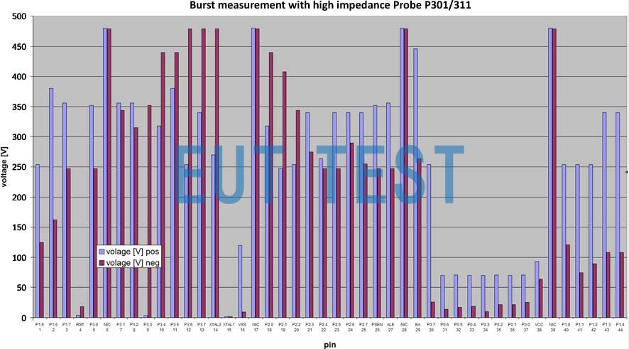
Fig. 5 Conductivity sensitivity of microcontroller pins to disturbances affecting electronic board circuit networks
Figure 5Display IC pin sensitivity varies widely. If the pins are insensitive, the line network may be located on the surface of an electronic board that is not protected by a ground plane and not be affected by an electric field (Figure 5in > 400 volt levels) without any interference . If the pins are sensitive, even complete shielding of the line network through the ground plane may not be sufficient. The surface of the test point or the surface of the IC pins connected to the line network may be sufficient to absorb the interference current from the electric field. The surface area of the line network (only a few square millimeters) is large enough to cause IC interference due to electric fields. The crystal oscillator connection of a microcontroller may have such a high sensitivity that, for example (Figure 5(Levels approx. 1-2 volts)
Figure 6Shows the measurement setup for determining sensitivity to conducted disturbances. the IC pins can be individually contacted with special probes and a test pulse applied. The test pulse corresponds to the effect of an electric field (burst, ESD) on the circuit network of an electronic board.
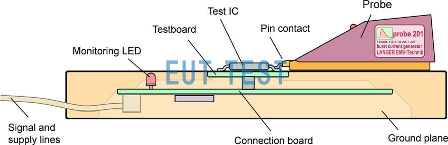
Fig. 6 Measurement setup for determining the sensitivity of the pins to conducted disturbances caused by electric fields on an electronic board
magnetic fields
The sensitivity of the IC pins to disturbing current pulses (bursts, ESD magnetic fields) can be determined in a similar way to theFigure 5is shown in the charts for . The currents associated with interference range from 0.5 to 35 amps. If the pins are sensitive, inductive loops of a few square millimeters are sufficient to cause inductive coupling. These loops can be formed by short sections of wire spaced 0.5 mm from the ground plane. Blocking capacitors may also form critical loops, especially if arranged at the edges of the electronics board. The highest magnetic field strength can usually be found there, which leads to the highest voltage induction.
If the electronic board has a ground system with slots (separated ground), magnetic fields may enter and induce voltages in the jumper network. This usually happens if the analog ground plane is separated from the digital ground plane. Only ground planes that are not separated and continuously connected can solve this problem. The power pins of crystal oscillators and PLL circuits are the most sensitive pins in practice. signal connections to ICs, such as reset, crystal oscillator, or test pins, can also be very sensitive.
In the early stages of electronic board development, it is beneficial to match the layout design and mechanical structure to the IC pin sensitivity. This increases the EMC immunity of the board. Today, IC manufacturers have measured the conducted sensitivity of IC pins.
- Created Date: 2024-08-26 10:38:25 ;
- Last modified on 2024-08-26 18:38:25 ;