EMC Requirements for Integrated Circuit Chips in Automotive Electronics
- Article Directory: How to test integrated circuits for electromagnetic compatibility
Preface:
EMC problems during the development of electronic modules for the automotive industry lead to very high development costs and loss of time. Therefore, the EMC requirements of automotive electronics for integrated circuit chips on-board chips need to meet certain standard limits.
Automotive electronic systems must meet ever-increasing performance requirements. This is why more and more highly integrated, ESD-sensitive ICs are being used in this field. As a result, ESD failures lead to an increasing number of malfunctions. These functional problems mainly affect highly integrated microcontrollers, where oscillator units and PLL units are very sensitive to ESD processes. Today's electronic applications do not even reach an ESD immunity of 2 kV in the worst case.
Chips are susceptible to interference when they have heat sinks
Experience has shown that applications with heat sinks on microcontrollers are particularly sensitive (Figure 1).
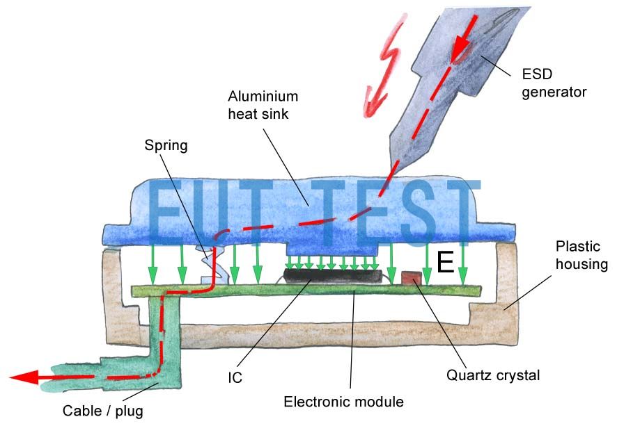
Fig. 1 Working principle behind ESD interference
Figure 1Shows the workings behind ESD interference. the ESD generator couples the interference pulse into the heat sink. This results in a voltage difference between the heat sink and the electronics module. This voltage difference creates an electrical interference field between the two components. The strength of the electric field is highest in the area of the heat sink because this is the area closest to the IC. This distance is actually in the range of about 0.2 to 1 mm. This high electric field strength may cause the IC to malfunction.
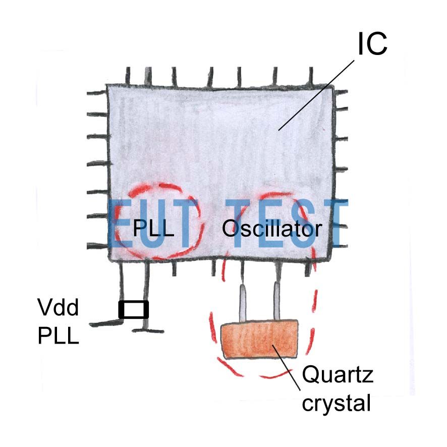
Fig. 2 Sensitive areas of the microcontroller detected with field sources
Examination of the IC with a manually guided electric field source reveals that the PLL and oscillator areas are particularly sensitive. the corresponding analysis of the IC failure confirms the PLL and oscillator failure.
groundFigure 1The ESD immunity can be assigned to the corresponding fault mode as shown in the example:
- 2 kV ESD for oscillator unit
- 3 kV ESD for PLL units
Shielding can be placed over the IC to ensure that no electric fields interfere with the IC (Figure 3). This will intercept the electric field emitted by the heat sink. In ESD testing, the shield must also extend over the quartz crystal.
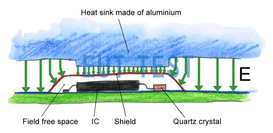
Fig. 3 Sensitive areas of the microcontroller detected with field sources
This precaution increases the ESD immunity to about 15 kV. It is not the shielding that determines the 15 kV limit, but other weak points in the electronic module. They are responsible for disturbances coupled to the IC via the line network simply by passing under the shielding.
ESD testing can only be performed on finished components. This means that all parts of the component and its production tooling have already been developed and produced. In our example, the common method of achieving EMC immunity by changing the board layout does not achieve the desired goal. The ESD interference originating from the heat sink acts directly on the IC housing. This problem can only be solved by changing the mechanical design. This means that the mechanical components have to be replaced and therefore the tools used for production have to be changed. This is an expensive method.
This problem can be avoided if the EMC characteristics of the IC are known before production.
There are two areas for action:
- IC manufacturers can improve ICs. this is already implemented in practice.
- Appropriate EMC precautions can be planned in the design of the mechanical structure.
Measurements are necessary to determine the EMC characteristics of the IC.

Fig. 4 Sensitive areas of the microcontroller detected with field sources
Figure 4Fig. 1 shows a measurement device for measuring the sensitivity of an electric field to an ESD pulse using an ESD generator. For this purpose, an electrode is arranged above the IC on which the tip of the ESD generator is placed. When an ESD pulse is applied, a corresponding electric pulse field is generated between the electrode and the test plate.The immunity of the IC can be determined by increasing the voltage of the ESD generator. This process is not very precise because the electric field pulses are highly dependent on the type and location of the ESD generator. For example, the pulse edges of an ESD generator can be superimposed on ESD generator-specific transients. The waveform of the pulse can also be altered by tilting the ESD gun, for example. In addition, stray fields can emerge from the generator and interfere with the IC uncontrollably.
Figure 5Shows a defined process.
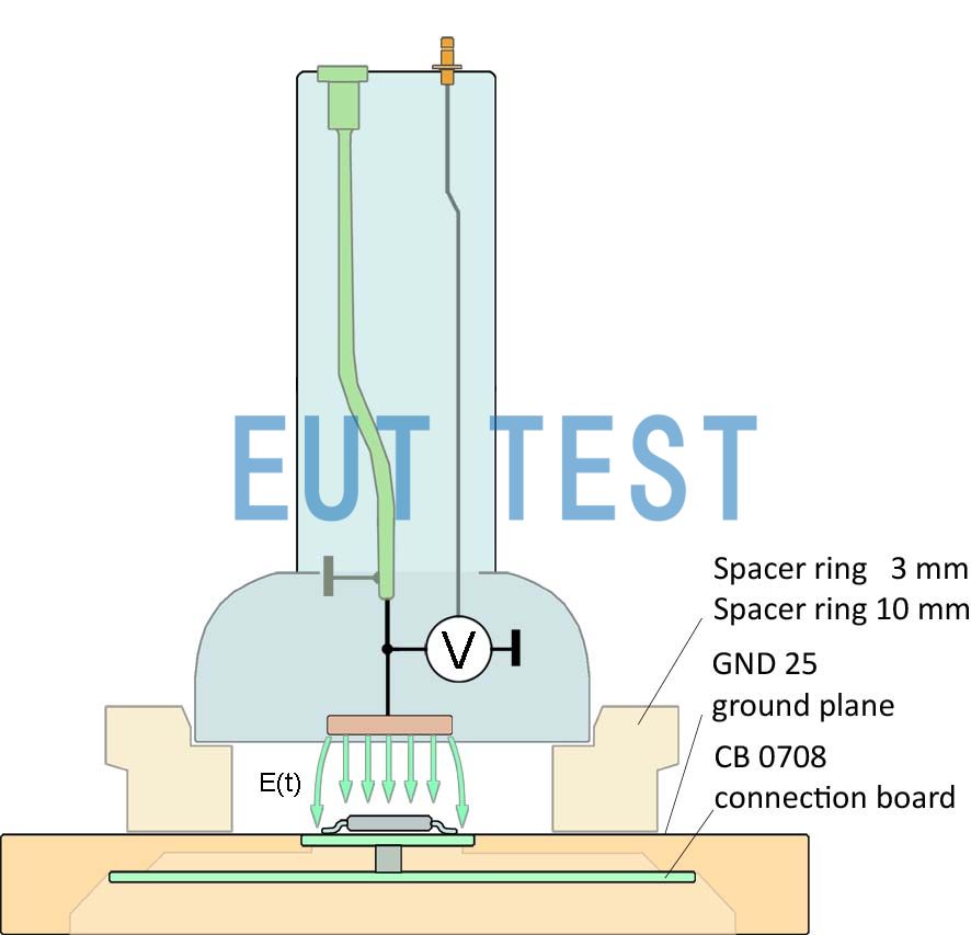
Fig. 5 Measurement setup using ESD generator
During testing, the IC is located in a shielded space formed by a ground plane, isolation ring, and field source. The field source is arranged at a defined height above the IC using the isolation ring. The field source consists of an electrode to which a test voltage pulse is applied. The electrodes generate a defined electric field in which the IC is located. The field source can be used to generate a variety of test pulses that may occur in practice. Rise times of 200 ps, 1ns, and 5ns may occur in practice. Increase the electrode voltage until the immunity of the IC is reached.
During an ESD event, additional magnetic fields may be generated by structural components, which may also interfere with the IC in practice. the same measurement setup and magnetic field source can be used to determine the magnetic field immunity level of the IC. The failure mode of the IC must be analyzed during these measurements.Table 1Microcontroller ESD immunity measurements as a function of disturbance pulse rise time are listed.
| 200 p seconds | 1 n second | 5 n seconds | |
| radical in Chinese characters (Kangxi radical 5) | 1,4 kV | 1,8 kV | 6,0 kV |
| H | 2,8 kV | 3,0 kV | 7,0 kV |
| Table 1 | |||
The measurement setup described here allows the determination of the EMC parameters of the IC. The measurement results can be used to plan the corresponding design modifications of the IC structure.
If an electric or magnetic field interferes with the IC from the outside, it is not appropriate to change the layout as a countermeasure. In this case, the only useful remedy is to change the mechanical design.
with regards toIn Figure 1The following countermeasures can be taken for the specific example of a heat sink on the IC that generates a strong electric field:
- Increase the number of contact springs between the electronics module and the heat sink
- Arrange a localized shield on the IC.Figure 3
- If possible, enclose the module in a shielded enclosure (perhaps using a feed-through filter)
- Move IC to side without field (can't be cooled)
- Increase clearance between IC and heat sink
Item 1)Contact springs reduce the voltage difference between the heat sink and the printed circuit board. This is because the total inductance of the springs is reduced if several springs are arranged in parallel. In practice it may be necessary to install about 20 springs to achieve this. If the stray fields of the springs are arranged in unfavorable locations, they may interfere with the ICs; therefore, complex and thorough testing is required to determine favorable spring locations. However, reliable spring contact cannot be ensured if aluminum heat sinks are used. This means that aluminum heat sinks must also be tinned, which can be costly. At this point, IC shielding may be more cost-effective (see section2 articles).
(item 2)When arranging a localized shield above the IC, it is important to ensure that it also covers the quartz crystal (similar to theFigure 3). However, for example, quartz crystals can also be placed in regions where there is no field on the other side of the electronic module.
In addition, it must be ensured that the shielding components are suitable for the manufacturing process.
(item 3)If possible, metal shielding should enclose the entire module. This may prevent the use of plastic enclosures.
Item 4)It is possible to move the IC to an area free of fields, e.g. on the other side of the electronics module, if the IC does not necessarily need to be cooled. In this case, care should be taken that the presence of mesh metal parts may couple out magnetic fields that may interfere with the IC. The testing of the first sample will show whether the modification of the whole design for this purpose has been successful, which is later in the production process.
(Item 5)The theoretical possibility of increasing the gap between the heat sink and the IC would result in a lower electric field strength. At the same time, the heat transfer and cooling of the IC will become less effective.
In conclusion, it can therefore be said that it is very beneficial to know the ESD parameters of the microcontroller in advance in terms of time and cost savings for the development of immunity components. This means that the ESD parameters of the microcontroller must be measured. This information will allow the necessary countermeasures to be planned as early as possible during the development of the component in order to ensure that the whole assembly is not disturbed.
- Created Date: 2024-08-26 10:42:15 ;
- Last modified on 2024-08-26 18:42:15 ;